CCD and Slice Layout
Chip level
Below the layout of the CCID80 silicon is shown.
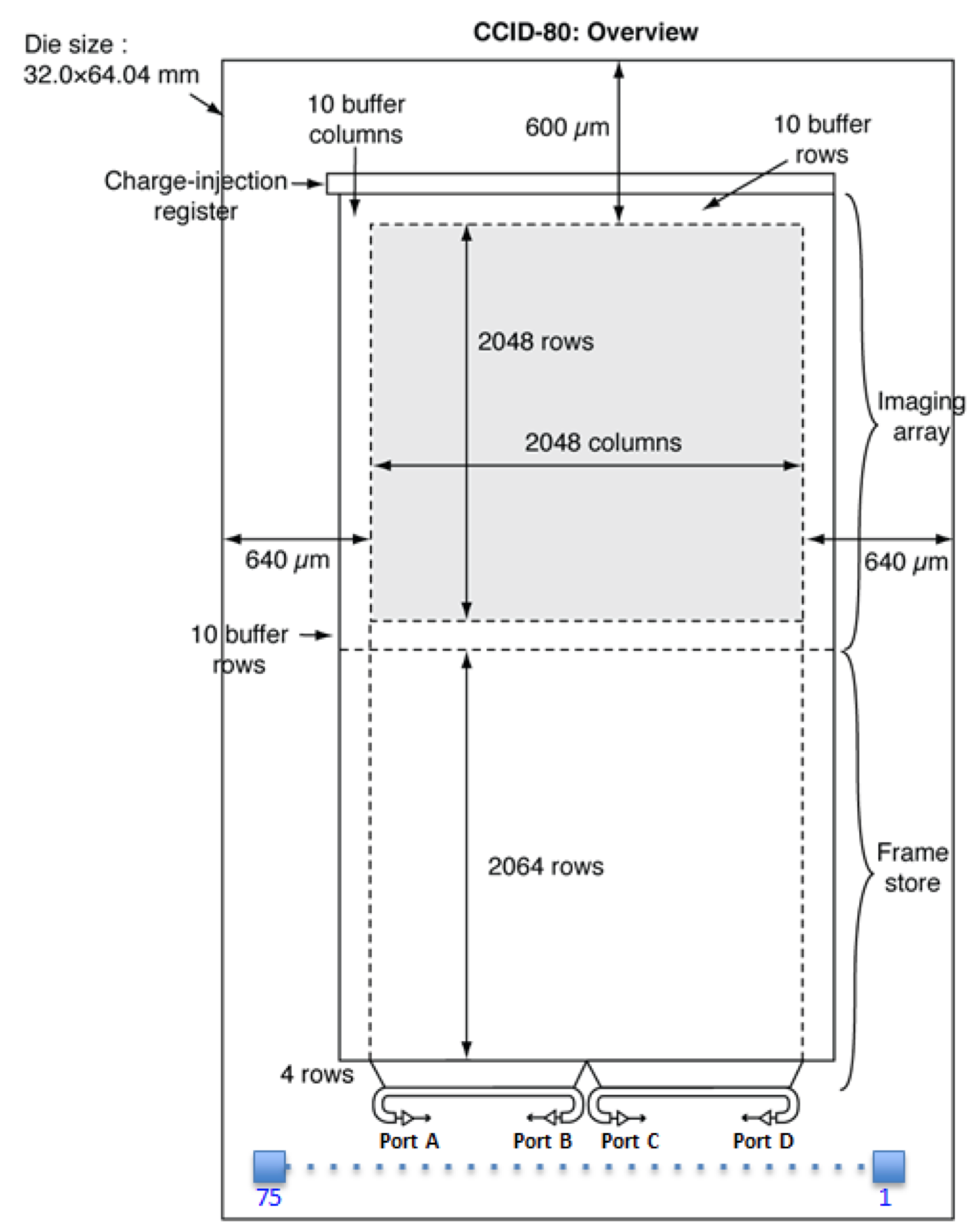
CCID80 Layout Diagram
Note that while the official imaging array is 2048 by 2048, there are addition buffer rows above and below that may also be used for imaging. The manufacturer asserts these rows are not as well calibrated given their proximity to the edge of the chip. Because TESS covers some of the lower buffer rows are covered with aluminum , these are not used. The upper buffer rows are readout with the rest of the image and no distinction is made.
The buffer columns do not connect to the output ports, so they do not appear in the data.
Not clearly shown in the CCID80 layout diagram is the
division of the imaging array and frame store into four slices.
Each slice has 512 columns. These are indexed by A through D here, and 0 through 3 throughout the code for httm.
There are 11 pre-scan pixels in the serial register between the bottom corner of the slice and its corresponding output port.
Note that output ports A and C are on the left edges of their slices while B and D are on the right edges of their slices. A consequence of this is that the electronics read pixels from rows in the A and C slices left to right, but those in the B and D slices right to left (in all cases, the electronics read rows from bottom to top in these diagrams).
Slice Level
Slice level refers to the data taken from a specific port through a measurement chain to its associated Analogue To Digital Converter (ADC).
It is important to understand how slice level functions electrically for simulation and calibration.
Each slice has its own measurement chain and ADC.
The slice diagram below depicts the format of the data output by the ADC.
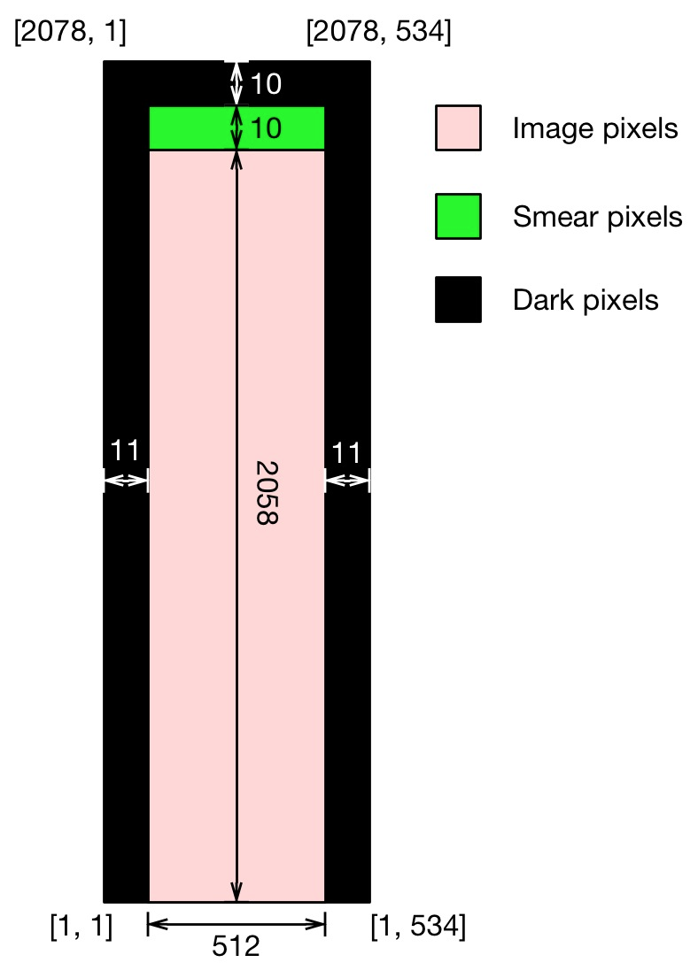
Slice Diagram
The lower buffer rows from the CCID80 layout digram are not included in the raster. Their charge is cleared prior to readout of the individual pixels. This is because some of these rows are covered with silicon and not exposed to significant amounts of light.
The upper buffer rows from the CCID80 layout diagram are included and no special distinction is made between them and the other image pixels.
The area labeled smear pixels in the slice layout are only exposed to light during the frame transfer time. They measure the excess charge in a column due to the unwanted exposure during frame transfer.
The dark pixels are never exposed to light, and are used to measure video bias.
Raw FITS Representation of Full Frames
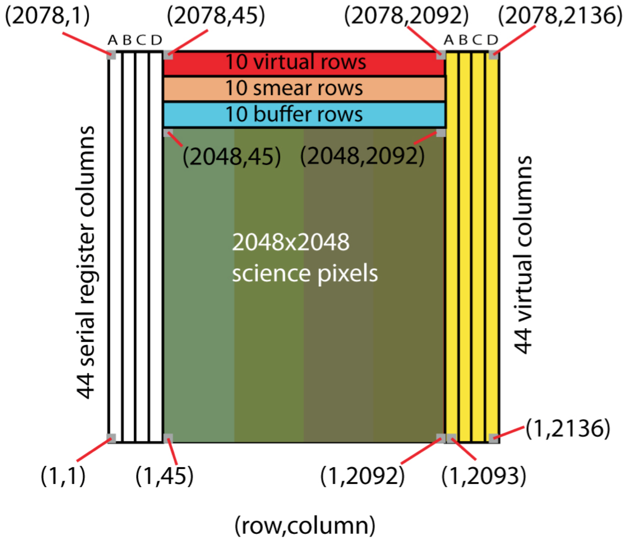
Raw FITS Layout Diagram
In the Raw FITS layout diagram, the following columns refer to each of the four slices:
- Slice A: 1..11, 45..556, 2093..2103
- Slice B: 12..22, 1068..557, 2104..2114
- Slice C: 23..33, 1069..1580, 2115..2125
- Slice D: 34..44, 2092..1581, 2126..2136
Remember that in httm Slice A is indexed as Slice 0, Slice B is indexed as Slice 1, C as 2, and D as 3.